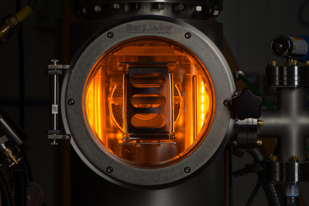
Epitaxy on demand
At our institute, we excel in providing bespoke solutions in the realm of III-V semiconductor epitaxy. Utilizing cutting-edge equipment, we bridge the gap between research and industry by enabling pilot series production of advanced devices for power and high-frequency electronics, as well as semiconductor lasers.
Our expertise in wafer epitaxy allows us to offer a comprehensive suite of services, including:
- Custom epitaxy of specific layer structures tailored to your requirements
- Development and small-scale production of epitaxial layers
- Expert scientific consultation
- Thorough characterization and analysis of grown layer structures
Partner with us to leverage our state-of-the-art technology and in-depth knowledge, driving innovation in your projects and pushing the boundaries of what’s possible in high-tech applications.

Our epitaxy offer for up to 2 inch wafers:
Laser structures (emission wavelenght 650 nm to 15 µm)
- Diode lasers (GaAs 750-1080 nm and GaSb 1800-2400 nm)
- Quantum Cascade lasers (QCL 3000-15000 nm)
- VECSEL
THz emitters and detectors
Detectors
- Shortwave IR: InGaAs and extended InGaAs
- Mid- and longwave IR: Type-II-SL, QWIP, avalanche
- Ultra-fast detectors
Electronics
- III-V based pHEMT, mHEMT
- Ultrafast transistors.
SESAME
Antimony-based templates
Others upon request. We can use our developed growth procedures or grow according to customers.
Our MBE reactor:
VEECO GENXplor R&D MBE system:
- 2’’ wafers;
- Extremely high composition and thickness accuracy (error <1.5%);
- Group III: In, 2xGa, Al;
Group V: As cracker, Sb cracker, Bi;
Dopants: Si, Be, Te (GaTe)
